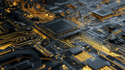
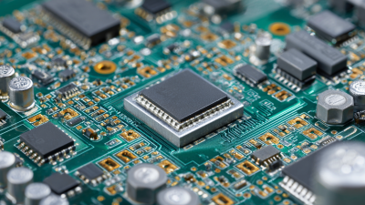
In the rapidly evolving landscape of electronics manufacturing, the significance of an optimized PCB process cannot be overstated. According to a report by the IPC, the global printed circuit board (PCB) market is expected to reach $76 billion by 2024, driven by trends such as miniaturization and increased demand for advanced electronics. Enhanced PCB processes not only provide higher quality and reliability but also optimize production efficiency and cost-effectiveness, essential for staying competitive in the market. As manufacturers adopt innovative techniques and technologies, from automation to advanced materials, the advantages gained can lead to improved product performance and reduced time to market. This blog will delve into the various benefits and practical applications of advanced PCB processes, demonstrating how they can unlock new possibilities for stakeholders in the electronics industry.

In the rapidly evolving electronics manufacturing landscape, improved PCB (Printed Circuit Board) processes are becoming essential for enhancing productivity and ensuring product quality. One major benefit of these advanced processes is the reduction in error rates during production. Automated techniques and better design tools lead to more precise manufacturing, minimizing defects that could compromise the functionality of electronic devices. As a result, manufacturers can anticipate fewer reworks and lower material waste, directly affecting their bottom line.
Another significant advantage is the acceleration of time-to-market for new products. Streamlined PCB processes enable faster prototyping and production cycles, allowing companies to respond swiftly to market demands and technological advancements. This agility not only enhances competitiveness but also promotes innovation within organizations. Furthermore, improved PCB processes often incorporate advanced materials and technologies that can lead to lighter, more efficient products, meeting the rising consumer expectations for performance and sustainability in electronics.
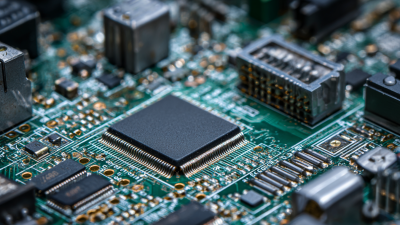
In the rapidly evolving landscape of electronics manufacturing, the choice between traditional and enhanced PCB manufacturing techniques can significantly impact both production efficiency and product quality. Traditional methods often rely on time-consuming, manual processes that are susceptible to human error. According to a report by IPC, traditional PCB manufacturing can result in a defect rate as high as 10%. In contrast, enhanced techniques, such as laser direct imaging (LDI) and automated optical inspection (AOI), have demonstrated a remarkable reduction in defect rates, often dropping below 1%.

Furthermore, the speed of production is another crucial differentiator. Enhanced PCB processes can reduce the average cycle time by up to 30%, as stated in a study by TechSearch International. This increased efficiency not only allows for rapid prototyping but also enables manufacturers to respond swiftly to market demands, thereby enhancing their competitive edge. Additionally, the adoption of advanced materials and techniques in enhanced PCB manufacturing contributes to better electrical performance and thermal management, making them a more viable choice for high-frequency and high-density applications.
As the complexity of electronic devices continues to grow, the necessity for robust and reliable PCB manufacturing techniques becomes paramount. Embracing enhanced methodologies not only streamlines the production process but also ensures high standards of quality, ultimately leading to better products that meet the rigorous demands of today's technology-driven market.
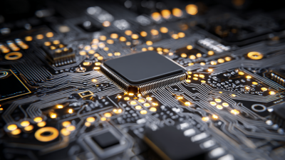
The advancements in PCB manufacturing processes are significantly transforming the landscape of electronics manufacturing. According to the IPC’s International Technology Roadmap for Electronic Components, the demand for high-density interconnect (HDI) PCBs is projected to grow at a CAGR of 12% through 2025. This surge is driven by the increasing complexity of electronics requiring smaller, lighter, and more efficient circuitry. Key technologies such as laser drilling and automated optical inspection (AOI) are enhancing the precision and reliability of PCB production, enabling manufacturers to meet these demands effectively.

Moreover, the integration of advanced materials like high-frequency laminates and lead-free solder is revolutionizing PCB design and performance. A report from ResearchAndMarkets highlights that the global market for advanced PCB materials is expected to reach $15.5 billion by 2027, with a strong focus on environmentally sustainable materials. These innovations not only improve electrical performance but also contribute to the industry’s shift towards greener manufacturing practices, aligning with regulatory requirements and consumer preferences. As these technologies continue to evolve, they pave the way for the development of next-generation electronic products that can cater to the intricate demands of various applications across industries.
The enhancement of PCB processes has emerged as a game-changer in electronics manufacturing, particularly in terms of cost-effectiveness. According to the IPC's "Global Technology Adoption" report, modern PCB processes have increased production efficiency by up to 30%, allowing manufacturers to reduce operational costs significantly. This efficiency not only lowers the production time but also minimizes material waste, which is crucial in an industry where margins are often razor-thin.
Moreover, updated manufacturing technologies such as automated soldering and advanced inspection systems contribute to enhanced quality control, lowering defect rates by nearly 50% as per a recent study by Gartner. These improvements not only save immediate costs but also enhance the overall reliability of electronic components, reducing long-term warranty and replacement expenditures. With cost savings in raw materials and increased yield rates, manufacturers can reallocate resources towards innovation and product development, making it clear that upgraded PCB processes are not just a necessity but a strategic advantage in the competitive global market.
| Dimension | Conventional PCB Process | Enhanced PCB Process | Cost Reduction (%) |
|---|---|---|---|
| Material Cost | $50,000 | $40,000 | 20% |
| Production Time (days) | 15 | 10 | 33% |
| Labor Cost | $30,000 | $25,000 | 16.67% |
| Defect Rate (%) | 5% | 2% | 60% |
| Total Cost | $80,000 | $65,000 | 18.75% |
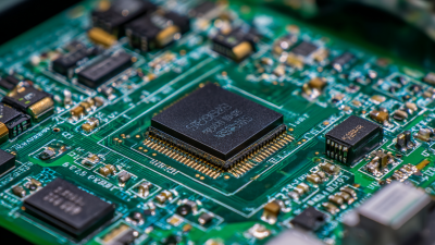
The modern electronics industry faces increasing pressure to adopt sustainable practices in manufacturing, particularly in the production of printed circuit boards (PCBs). Enhanced PCB manufacturing methods not only improve performance efficiency but also significantly reduce harmful environmental impacts. By integrating eco-friendly materials and optimizing production processes, manufacturers can minimize waste and energy consumption, contributing to a greener future.
One notable sustainable approach is the use of lead-free solder and recyclable materials, which comply with global environmental regulations. Moreover, advanced techniques like additive manufacturing allow for more precise material usage, reducing excess waste traditionally generated in subtractive processes. These innovations ensure that the lifecycle of PCBs aligns with sustainability goals while maintaining the high quality and reliability demanded by today’s electronic applications.
Investing in enhanced PCB manufacturing methods also opens the door to improved resource management and operational efficiency. By adopting practices that focus on sustainability, manufacturers not only comply with increasingly stringent regulations but also appeal to a growing consumer base that values environmentally responsible products. Embracing these methods is not just a trend but a necessary evolution toward a more sustainable and responsible electronics industry.
„Thanks to the LUVIR technology, the solder resist process could be switched directly from the previously used mask exposure to direct exposure. As an outstanding digital solution on the market, this technology has been able to demonstrate fast process times and superior quality on our certified conventional ink in production. This allowed us to fully digitize the solder mask process at low cost – without process or ink adjustments. An excellent benefit to our production in Rot am See.“
Ralf Göhringer (Head of Production WE Rot am See)
I would definitely recommend the Limata machine and team for a future company purchase
Michael Greenaway
Compunetics Inc.
“The Limata ldi has been amazing!! Best thing we did was buy this machine”
Richard Brady
GM
Circuitlabs
“Since 2019, we have been running the Limata X1000 LDI system (including LUVIR for solder mask imaging) in daily production as an addition to our current process with film. The machine was capable of properly exposing Taiyo PSR-4000 BN (DI) solder mask types on normal to high-copper boards using a new and unique direct imaging process. The machine operating interface is very user friendly which allowed for a quick technical training curve. The pre-registration processing reduced several seconds of production time at every print. Limata support and service staff is incomparable. They supported our team every step of the way at basically any time of the day or night, with literally, an immediate response time, customizing the software interface to best fit our Operations and needs.
We have exposed more than 8,000 prints since end of October, on various solder mask colors and some resist film panels. Limata, has proven to be very capable and innovative. They are a strong contender in the industry.
We have very much enjoyed this project, and working with the team!
Thank you Limata for the continued support and being a part of our growth.”
Bill Sezate
Vice President, GM
Summit Interconnect
As a replacement to our current contact exposure process with film, the LIMATA X2000 system including LUVIR-Technology was capable of properly exposing non-LDI solder mask types using a direct imaging process. The machine offers cutting edge software with a very intuitive operating interface which allowed for quick technician training curve. The dual drawer system combined with pre-registration processing reduced several seconds of production time at every machine cycle. Limata support and service staff is world class. They added software patches to keep production running at shortest possible response times, customized the software interface to best fit our in-house Operations system, and even wrote a step-by-step machine processing manual. As a result of the project, we have exposed more than 16,000 times on various product types and solder mask brands/colors. Limata, in a very short timeframe as a company, has definitely shown they are truly innovative and will be challenging the industry of direct imaging for the top spot.
Kevin Beattie
Process Engineer
TTM Technologies
Forest Grove Division