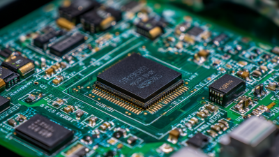
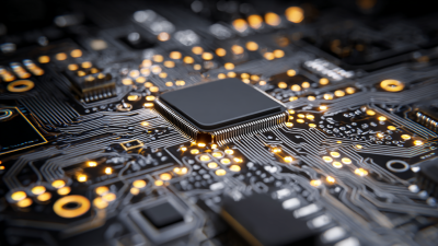
In the ever-evolving world of electronics, the PCB process stands as a critical foundation for creating reliable and efficient devices. As technology advances, the demand for complex and high-performance printed circuit boards (PCBs) intensifies, leading to a host of challenges that manufacturers must navigate. From design intricacies and material selection to production methods and quality assurance, each stage of the PCB process presents unique obstacles that can significantly impact the final product. This ultimate guide aims to illuminate these challenges and provide actionable solutions, equipping designers and engineers with the knowledge needed to optimize their PCB production journey.

Whether you're a seasoned professional or new to the field, understanding these dynamics is essential for achieving success in an increasingly competitive landscape. Join us as we explore the intricacies of the PCB process and unveil strategies to overcome its hurdles.
In the world of PCB (Printed Circuit Board) design, several challenges can arise, often leading to critical pitfalls in the process. One common issue is the lack of comprehensive data insights, which can hinder effective decision-making. Designers may overlook essential factors such as signal integrity, thermal management, and component placement during the initial design phase. This oversight can result in boards that are not just difficult to manufacture, but also underperform in real-world applications. Therefore, integrating data analytics into the design process can help identify potential problems earlier and streamline workflows.
Another prevalent pitfall in PCB design is the underestimation of production tolerances and manufacturing constraints. Many designers might focus exclusively on functionality, neglecting the specifications required for successful fabrication. For instance, tight pitch components could lead to challenges in soldering and assembly, while inappropriate layer stack-ups may result in signal loss or interference. By prioritizing collaboration with manufacturing partners and thoroughly understanding their capabilities, designers can better align their designs with practical constraints, ultimately leading to more reliable and efficient PCBs.
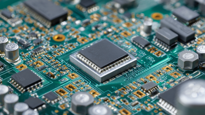
Manufacturing defects in printed circuit boards (PCBs) can significantly impact product quality, leading to increased costs and delays in delivery. Statistics indicate that a substantial percentage of PCBs experience defects during production, ranging from soldering issues to component misalignment. Understanding these challenges is critical for engineers aiming to optimize the PCB production process. By implementing rigorous quality control measures and advanced inspection techniques, manufacturers can substantially reduce the occurrence of defects, ensuring a greater reliability of the final product.
One effective solution lies in leveraging in-circuit testing methods, which focus on validating each component's functionality within the PCB. This approach not only identifies defects early in the assembly process but also enhances the overall integrity of the circuit board. Additionally, employing precise PCB measurement techniques can further ensure that quality standards are met, minimizing the risk of defects attributable to measurement errors. As technology continues to advance, adopting these methods will prove essential in achieving zero defects in PCB production, resulting in higher customer satisfaction and reduced production costs.

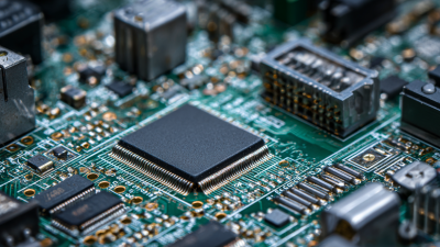
Quality control is a critical aspect of PCB assembly that directly impacts the reliability and performance of electronic devices. To mitigate risks associated with assembly defects, implementing best practices is essential. One effective strategy is to incorporate automated inspection systems, such as Automated Optical Inspection (AOI) and X-ray inspections. These technologies help in detecting issues like misaligned components, solder joint integrity, and surface defects before they escalate into more significant problems.

Another vital practice is to establish a thorough testing protocol throughout the assembly process. This includes functional testing and in-circuit testing, which can identify faults early on. Additionally, utilizing robust process controls during assembly ensures that each step is monitored closely. Regular training for assembly line workers on the latest techniques and equipment can enhance their skills and awareness, further reducing the risk of errors. By maintaining a strong focus on quality control, manufacturers can not only enhance product reliability but also improve customer satisfaction, ultimately leading to better market competitiveness.
Cost management in PCB processes is a critical concern for manufacturers, especially as the industry grapples with rising material costs and global competition. According to a recent IPC report, the average cost of raw materials in PCB manufacturing has increased by over 30% in the past few years, significantly impacting profit margins. To combat these challenges, companies are adopting several strategies to optimize their processes and reduce costs.
One effective approach is the implementation of advanced manufacturing techniques, such as automation and lean manufacturing principles. By streamlining operations, manufacturers can minimize waste and improve efficiency. A study by McKinsey & Company indicates that manufacturers who embrace automation can reduce production costs by up to 20%, thus providing a substantial buffer against rising material prices. Additionally, engaging in collaborative supply chain management can lead to bulk purchasing discounts and better inventory control, ensuring that firms can secure the materials they need at lower prices.
Furthermore, investing in design optimization tools can significantly reduce costs associated with PCB production. According to a report from Gartner, companies that utilize software for Design for Manufacturability (DFM) can lower overall production costs by as much as 15% by identifying potential issues early in the design stage. By focusing on cost-efficient design and manufacturing practices, PCB manufacturers can sustain profitability while navigating the complexities of market demands and cost fluctuations.
Emerging technologies are transforming the landscape of PCB (Printed Circuit Board) development, providing innovative solutions to age-old challenges. One significant advancement is the rise of additive manufacturing, commonly known as 3D printing. This technology allows for the rapid prototyping of PCBs, enabling designers to create intricate designs with reduced waste and faster turnaround times. The ability to print circuits directly onto substrates opens up possibilities for more complex and lightweight designs, catering to the demands of compact electronic devices.
Another noteworthy innovation is the integration of flexible and stretchable materials in PCB manufacturing. These advanced materials not only improve the durability of PCBs but also expand their applications in wearable technology and medical devices. By creating boards that can bend and stretch without losing functionality, manufacturers can enhance user comfort and device performance. Furthermore, advancements in AI and machine learning are optimizing the design and testing phases, reducing errors and time to market. These technological trends are not just reshaping the PCB industry but also paving the way for smarter and more efficient electronic products in various sectors.
| Challenge | Impact | Emerging Solution | Impact of Solution |
|---|---|---|---|
| High Production Costs | Limitations on scalability and profitability | Automation and AI in production | Reduction in labor costs and increased efficiency |
| Design Complexity | Increased likelihood of errors and delays | Advanced CAD tools and simulation | Improved design accuracy and reduced time-to-market |
| Material Limitations | Compromised performance and durability | Use of flexible and composite materials | Enhanced performance in various applications |
| Supply Chain Disruptions | Delays in production and delivery | Blockchain for supply chain transparency | Improved reliability and visibility in procurement |
| Environmental Regulations | Increased compliance costs | Green materials and processes | Lower environmental impact and compliance with regulations |
„Thanks to the LUVIR technology, the solder resist process could be switched directly from the previously used mask exposure to direct exposure. As an outstanding digital solution on the market, this technology has been able to demonstrate fast process times and superior quality on our certified conventional ink in production. This allowed us to fully digitize the solder mask process at low cost – without process or ink adjustments. An excellent benefit to our production in Rot am See.“
Ralf Göhringer (Head of Production WE Rot am See)
I would definitely recommend the Limata machine and team for a future company purchase
Michael Greenaway
Compunetics Inc.
“The Limata ldi has been amazing!! Best thing we did was buy this machine”
Richard Brady
GM
Circuitlabs
“Since 2019, we have been running the Limata X1000 LDI system (including LUVIR for solder mask imaging) in daily production as an addition to our current process with film. The machine was capable of properly exposing Taiyo PSR-4000 BN (DI) solder mask types on normal to high-copper boards using a new and unique direct imaging process. The machine operating interface is very user friendly which allowed for a quick technical training curve. The pre-registration processing reduced several seconds of production time at every print. Limata support and service staff is incomparable. They supported our team every step of the way at basically any time of the day or night, with literally, an immediate response time, customizing the software interface to best fit our Operations and needs.
We have exposed more than 8,000 prints since end of October, on various solder mask colors and some resist film panels. Limata, has proven to be very capable and innovative. They are a strong contender in the industry.
We have very much enjoyed this project, and working with the team!
Thank you Limata for the continued support and being a part of our growth.”
Bill Sezate
Vice President, GM
Summit Interconnect
As a replacement to our current contact exposure process with film, the LIMATA X2000 system including LUVIR-Technology was capable of properly exposing non-LDI solder mask types using a direct imaging process. The machine offers cutting edge software with a very intuitive operating interface which allowed for quick technician training curve. The dual drawer system combined with pre-registration processing reduced several seconds of production time at every machine cycle. Limata support and service staff is world class. They added software patches to keep production running at shortest possible response times, customized the software interface to best fit our in-house Operations system, and even wrote a step-by-step machine processing manual. As a result of the project, we have exposed more than 16,000 times on various product types and solder mask brands/colors. Limata, in a very short timeframe as a company, has definitely shown they are truly innovative and will be challenging the industry of direct imaging for the top spot.
Kevin Beattie
Process Engineer
TTM Technologies
Forest Grove Division