In the rapidly evolving landscape of technology and manufacturing, China stands out as a key player, particularly in the realm of PCB solutions. As we head toward 2025, the integration of advanced technologies such as automation, IoT, and AI into the manufacturing processes is not just a trend, but a necessity for staying competitive on a global scale. This blog will explore the pivotal role that China’s manufacturing sector plays in delivering unmatched PCB solutions, emphasizing the importance of adapting to industry trends and innovations.

Furthermore, we will provide a checklist that companies can utilize to assess their readiness for these upcoming changes, ensuring they remain at the forefront of PCB technology. Join us as we delve into how this global partnership can drive your business forward in a future that promises ever-increasing complexity and opportunity.
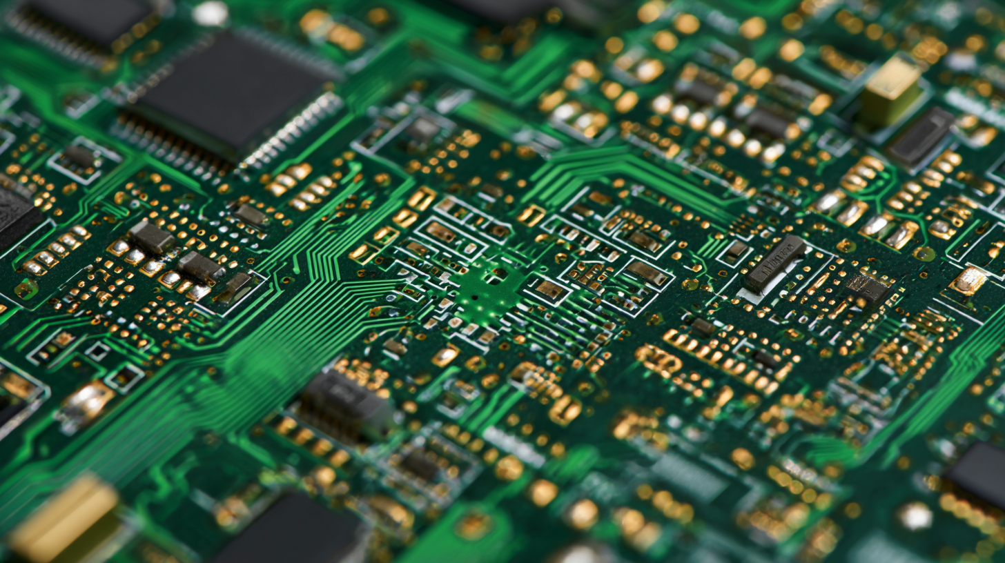
In today's fast-paced digital landscape, the demand for high-quality printed circuit boards (PCBs) in consumer electronics continues to soar. The semiconductor leadframe market is projected to experience significant growth driven by consumer demand for cutting-edge technology that offers faster internet access and enhanced functionalities. As lifestyles evolve with increased digitalization and the demand for luxury products rises, industries are urgently seeking PCB solutions that can meet these heightened expectations.
Real-world applications of PCBs are increasingly evident in various sectors, particularly in consumer electronics. Notably, the evolution in automotive technology showcased at CES 2025 highlights a shift among OEMs from traditional black-box solutions to modular architectures that enhance performance. This transition requires advanced PCBs capable of integrating multi-modal input data and context-aware machine learning to optimize sensor functionalities. With reports projecting a continuous demand for innovative and efficient consumer electronics, partnering with leading PCB manufacturers becomes crucial for companies aiming to stay competitive in the market while meeting the needs of tech-savvy consumers.
| Application Area | PCB Type | Layer Count | Material Used | Typical Thickness (mm) | Production Volume (Units/Month) |
|---|---|---|---|---|---|
| Smartphones | Multilayer PCB | 6 | FR-4 | 1.6 | 1,000,000 |
| Laptops | HDI PCB | 10 | FR-4, Rogers | 1.2 | 500,000 |
| Wearable Devices | Flexible PCB | 4 | Polyimide | 0.2 | 300,000 |
| Televisions | Multilayer PCB | 8 | FR-4 | 1.6 | 750,000 |
| Home Appliances | Single-Sided PCB | 1 | FR-4 | 1.6 | 1,200,000 |
In the rapidly evolving landscape of medical device manufacturing, the demand for innovative, high-quality printed circuit boards (PCBs) is paramount. According to a recent report from MarketsandMarkets, the global medical device market is projected to reach $612.7 billion by 2025, growing at a compound annual growth rate (CAGR) of 5.4%. This growth underscores the increasing necessity for reliable PCB solutions that cater to specific operational requirements in medical technology—from diagnostics to therapeutic devices.
China has positioned itself as a leader in providing unmatched PCB solutions tailored for medical applications. With advancements in technologies such as HDI (High-Density Interconnector) and flexible PCBs, manufacturers can achieve greater miniaturization and functionality in their devices. Industry data from IBISWorld indicates that the PCB manufacturing industry in China is valued at approximately $22.3 billion, driven by a robust domestic market and increasing export demand. These innovations directly correlate with improved patient outcomes, as precise and efficient PCBs are essential for the reliability and performance of medical devices. By leveraging China's manufacturing capabilities, companies can ensure that their devices meet rigorous standards while remaining competitive in pricing and production timelines.
As the automotive industry continues to evolve, the demand for advanced PCB designs is at the forefront of enhancing automotive technology. With the global assembly machine market projected to reach $889.9 million by 2025, and a forecasted growth to $1.587 billion by 2033, at a compound annual growth rate of 7.5%, innovation in PCB design plays a crucial role in meeting these industry needs. Power devices like MOSFETs and IGBTs require optimal packaging designs that focus on thermal management, efficiency, and reliability to prevent overheating and ensure performance longevity.
Tip: When designing PCBs for automotive applications, consider integrating advanced thermal management solutions. Effective thermal management not only helps enhance reliability but also significantly extends the operational lifespan of power devices.
Research indicates a significant shift towards silicon carbide (SiC) and gallium nitride (GaN) technologies, which are evaluated for their potential in optimizing system costs. As electric vehicles gain traction, addressing key concerns such as driving range and efficiency will be pivotal. Industry experts from various semiconductor companies have emphasized the importance of R&D in automotive-grade power semiconductor modules during conferences, reinforcing the urgent need for cutting-edge technology in this rapidly growing sector.
Tip: Stay abreast of the latest trends in semiconductor innovations, as these developments are crucial for enhancing your PCB design strategies and ensuring competitive performance in the automotive market.
In the rapidly evolving landscape of industrial automation and control systems, Printed Circuit Boards (PCBs) play a critical role in ensuring efficiency and reliability. As China’s premier manufacturer of innovative PCB solutions, our commitment extends beyond supply; we partner with industries to develop tailored solutions that meet the demands of modern automation. PCBs are integral to a multitude of applications, from robotics and process control to sensor networks, providing the backbone for seamless integration and communication between devices.
Our advanced PCB designs are engineered to handle the complexities of industrial environments. High-density interconnects and customized layouts enable us to optimize space and performance, allowing systems to operate with maximum efficiency. Furthermore, our manufacturing capabilities ensure that all products meet rigorous quality and compliance standards, ultimately enhancing the dependability of control systems in critical applications. By leveraging cutting-edge technology and expertise, we empower businesses to thrive in an increasingly automated world, solidifying our role as a trusted global partner in PCB solutions.

Sustainable practices in PCB (Printed Circuit Board) production are becoming increasingly vital as industries seek eco-friendly solutions. According to a report from the IPC (Institute for Printed Circuits), the global PCB market is projected to reach $83 billion by 2025, highlighting the importance of environmentally responsible manufacturing. With the rising awareness of environmental issues, manufacturers are obliged to adopt practices that minimize waste and reduce their carbon footprint.
In recent years, many leading PCB manufacturers have implemented green initiatives such as using biodegradable materials and adopting closed-loop water systems. A study by the Electronics Industries Alliance reported that companies reducing hazardous waste in PCB production can improve overall efficiency by about 20%. Furthermore, using advanced technologies such as LED UV curing can significantly lower energy consumption during the manufacturing process, aligning with the global shift towards renewable energy sources. Through these sustainable strategies, manufacturers not only contribute to environmental conservation but also cater to the growing demand for eco-friendly electronics.
„Thanks to the LUVIR technology, the solder resist process could be switched directly from the previously used mask exposure to direct exposure. As an outstanding digital solution on the market, this technology has been able to demonstrate fast process times and superior quality on our certified conventional ink in production. This allowed us to fully digitize the solder mask process at low cost – without process or ink adjustments. An excellent benefit to our production in Rot am See.“
Ralf Göhringer (Head of Production WE Rot am See)
I would definitely recommend the Limata machine and team for a future company purchase
Michael Greenaway
Compunetics Inc.
“The Limata ldi has been amazing!! Best thing we did was buy this machine”
Richard Brady
GM
Circuitlabs
“Since 2019, we have been running the Limata X1000 LDI system (including LUVIR for solder mask imaging) in daily production as an addition to our current process with film. The machine was capable of properly exposing Taiyo PSR-4000 BN (DI) solder mask types on normal to high-copper boards using a new and unique direct imaging process. The machine operating interface is very user friendly which allowed for a quick technical training curve. The pre-registration processing reduced several seconds of production time at every print. Limata support and service staff is incomparable. They supported our team every step of the way at basically any time of the day or night, with literally, an immediate response time, customizing the software interface to best fit our Operations and needs.
We have exposed more than 8,000 prints since end of October, on various solder mask colors and some resist film panels. Limata, has proven to be very capable and innovative. They are a strong contender in the industry.
We have very much enjoyed this project, and working with the team!
Thank you Limata for the continued support and being a part of our growth.”
Bill Sezate
Vice President, GM
Summit Interconnect
As a replacement to our current contact exposure process with film, the LIMATA X2000 system including LUVIR-Technology was capable of properly exposing non-LDI solder mask types using a direct imaging process. The machine offers cutting edge software with a very intuitive operating interface which allowed for quick technician training curve. The dual drawer system combined with pre-registration processing reduced several seconds of production time at every machine cycle. Limata support and service staff is world class. They added software patches to keep production running at shortest possible response times, customized the software interface to best fit our in-house Operations system, and even wrote a step-by-step machine processing manual. As a result of the project, we have exposed more than 16,000 times on various product types and solder mask brands/colors. Limata, in a very short timeframe as a company, has definitely shown they are truly innovative and will be challenging the industry of direct imaging for the top spot.
Kevin Beattie
Process Engineer
TTM Technologies
Forest Grove Division