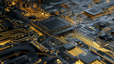
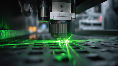
In recent years, the electronics manufacturing industry has witnessed a significant shift towards advanced imaging techniques, with laser direct imaging (LDI) emerging as a frontrunner in precision and efficiency. According to a report by MarketsandMarkets, the global LDI market is projected to grow at a compound annual growth rate (CAGR) of 7.6%, reaching USD 750 million by 2025. This innovation allows for the direct transfer of digital images onto substrates without the need for traditional phototools, leading to reduced costs and improved turnaround times.

The benefits of laser direct imaging extend beyond mere production efficiency; they include enhanced design flexibility and the capability to produce finer features required for modern electronics, such as those found in high-density interconnect (HDI) printed circuit boards. As industries continue to seek more innovative solutions to meet the increasing demands for miniaturization and complexity in electronic devices, LDI stands out as a pivotal technology that promises to reshape the landscape of manufacturing processes.
 Laser Direct Imaging (LDI) is revolutionizing manufacturing processes, leveraging emerging technologies to enhance precision and efficiency. As industries seek to innovate, advancements in laser systems, software, and materials are paving the way for more capable LDI applications. With improved image resolution and speed, businesses can produce high-quality products while significantly reducing waste.
One promising technology in this field is the integration of artificial intelligence (AI) into LDI systems. By utilizing AI, manufacturers can optimize laser settings and adapt in real-time to variations in substrate and material properties. This not only improves accuracy but also accelerates production times.
Tip: When implementing AI solutions in LDI, ensure your team is trained on the software's capabilities to fully harness its potential.
Another key advancement is the development of specialized laser wavelengths tailored to different materials. This specificity allows for better bonding and less thermal stress on substrates, resulting in higher fidelity images.
Tip: Stay updated on the latest laser technology developments to select the best solutions for your specific manufacturing needs. By adopting these innovative tools, companies can transform their LDI processes and maintain a competitive edge in the market.
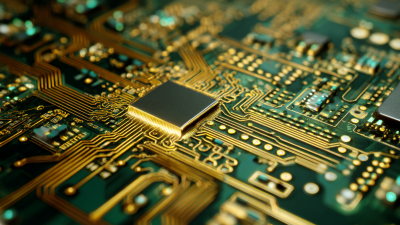
Laser Direct Imaging (LDI) technology is revolutionizing the way circuit boards are manufactured, offering several key advantages over traditional photolithography methods. One of the most significant benefits is the precision it provides. According to a report by Research and Markets, the global market for LDI is projected to grow at a CAGR of 8.6% between 2021 and 2026. This growth is largely attributed to the superior resolution and reduced line widths that LDI can achieve, often down to 5 microns or less, compared to 20 microns for conventional methods. Such precision enhances the performance of high-density interconnect (HDI) circuits, crucial for advanced electronic devices.
Additionally, LDI boasts a higher throughput and lower production costs due to reduced material waste and shorter processing times. A study from the Institute of Electrical and Electronics Engineers (IEEE) highlights that LDI can cut overall manufacturing costs by up to 30% through its ability to eliminate the need for masks and extensive chemical processing involved in traditional techniques. This efficiency not only streamlines production but also supports environmentally sustainable practices, making LDI an attractive option for manufacturers aiming to reduce their ecological footprint while meeting the growing demand for complex and compact electronic components.

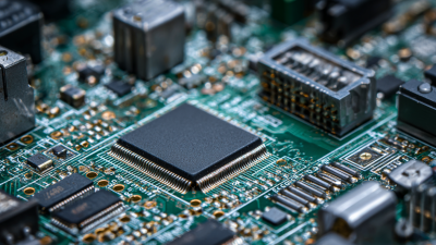
The implementation of innovative Laser Direct Imaging (LDI) solutions has been transformative for various industries, providing notable precision and efficiency in production processes. Recent case studies showcase how companies have successfully integrated LDI technologies into their operations, yielding impressive results in quality and throughput. These advancements not only reduce production times but also minimize material waste, making them a sustainable choice for modern manufacturing.
One significant case highlights a manufacturer that adopted LDI to enhance its printed circuit board (PCB) production. By utilizing LDI, they achieved sharper imaging and increased component density, which led to improved performance of their electronic devices. This success illustrates the potential of LDI to push the boundaries of design and fabrication in electronics. Additionally, as industries increasingly face the need for sustainable practices, LDI’s ability to optimize the use of materials aligns perfectly with the growth of eco-engineering approaches, akin to restoring estuarine ecosystems through innovative solutions. Such synergies emphasize the importance of ongoing research and collaboration in driving forward both technology and environmental stewardship.
| Application Type | Industry | Challenge | Solution Implemented | Results Achieved |
|---|---|---|---|---|
| PCB Manufacturing | Electronics | High precision required for intricate designs | Advanced Laser Direct Imaging technology | Improved accuracy by 30%, reduced waste by 20% |
| Printed Circuit Boards | Telecommunications | Time-consuming traditional methods | Integration of Laser Direct Imaging | Reduced production time by 50% |
| Microelectronics | Consumer Electronics | Need for high-resolution patterns | Utilization of high-resolution laser systems | Enhanced resolution, increasing yield by 25% |
| Double-sided PCBs | Automotive | Inaccuracies in layer alignment | Real-time alignment with Laser Direct Imaging | Eliminated misalignments, improving reliability |
| High-Density Interconnect (HDI) | Aerospace | Complex multilayer structures | State-of-the-art laser imaging solutions | Achieved tighter tolerances, enhancing performance |
As we move deeper into the digital age, Laser Direct Imaging (LDI) technology is poised to revolutionize a variety of industries. The future of LDI is marked by immense potential for enhanced precision and efficiency. Expect to see advancements in resolution and speed, allowing for more intricate designs and faster production times. Innovations such as artificial intelligence and machine learning will likely play a significant role in optimizing LDI processes, making them more adaptable to different applications.
Tip: Stay updated on emerging trends by attending industry conferences and webinars, as they often showcase the latest technological advancements and case studies in LDI. Networking with experts can also provide insights into practical applications of these innovations.
Additionally, sustainability is anticipated to be a critical focus in the coming years. The push for eco-friendly practices will drive the development of LDI systems that reduce waste and energy consumption. Companies that prioritize green technologies will not only comply with regulations but also attract eco-conscious clients.
Tip: Invest in sustainability training for your team to better align with these future trends, ensuring that your business remains competitive and socially responsible in the evolving market.
The adoption of Laser Direct Imaging (LDI) technology presents several challenges that industry players must navigate to fully harness its benefits. One of the primary obstacles is the initial cost of investment, as LDI systems can be significantly more expensive than traditional imaging methods. This hefty price tag can deter manufacturers from making the switch, particularly if they are operating on tight budgets. Furthermore, there is a steep learning curve associated with integrating LDI into existing workflows, requiring specialized training for personnel to ensure optimal operation.
On the technical side, achieving high-quality imaging while maintaining productivity levels can be a daunting task. LDI technology demands precise calibration and tuning to produce accurate patterns and resist profiles, which can lead to increased setup times. Additionally, manufacturers must address potential issues such as alignment consistency and the management of different substrate materials. To overcome these hurdles, developing innovative software solutions that streamline workflow processes and enhance machine compatibility will be crucial in facilitating a smoother transition to LDI technology. By addressing both the economic and technical challenges head-on, companies can position themselves for success in this rapidly evolving landscape.


„Thanks to the LUVIR technology, the solder resist process could be switched directly from the previously used mask exposure to direct exposure. As an outstanding digital solution on the market, this technology has been able to demonstrate fast process times and superior quality on our certified conventional ink in production. This allowed us to fully digitize the solder mask process at low cost – without process or ink adjustments. An excellent benefit to our production in Rot am See.“
Ralf Göhringer (Head of Production WE Rot am See)
I would definitely recommend the Limata machine and team for a future company purchase
Michael Greenaway
Compunetics Inc.
“The Limata ldi has been amazing!! Best thing we did was buy this machine”
Richard Brady
GM
Circuitlabs
“Since 2019, we have been running the Limata X1000 LDI system (including LUVIR for solder mask imaging) in daily production as an addition to our current process with film. The machine was capable of properly exposing Taiyo PSR-4000 BN (DI) solder mask types on normal to high-copper boards using a new and unique direct imaging process. The machine operating interface is very user friendly which allowed for a quick technical training curve. The pre-registration processing reduced several seconds of production time at every print. Limata support and service staff is incomparable. They supported our team every step of the way at basically any time of the day or night, with literally, an immediate response time, customizing the software interface to best fit our Operations and needs.
We have exposed more than 8,000 prints since end of October, on various solder mask colors and some resist film panels. Limata, has proven to be very capable and innovative. They are a strong contender in the industry.
We have very much enjoyed this project, and working with the team!
Thank you Limata for the continued support and being a part of our growth.”
Bill Sezate
Vice President, GM
Summit Interconnect
As a replacement to our current contact exposure process with film, the LIMATA X2000 system including LUVIR-Technology was capable of properly exposing non-LDI solder mask types using a direct imaging process. The machine offers cutting edge software with a very intuitive operating interface which allowed for quick technician training curve. The dual drawer system combined with pre-registration processing reduced several seconds of production time at every machine cycle. Limata support and service staff is world class. They added software patches to keep production running at shortest possible response times, customized the software interface to best fit our in-house Operations system, and even wrote a step-by-step machine processing manual. As a result of the project, we have exposed more than 16,000 times on various product types and solder mask brands/colors. Limata, in a very short timeframe as a company, has definitely shown they are truly innovative and will be challenging the industry of direct imaging for the top spot.
Kevin Beattie
Process Engineer
TTM Technologies
Forest Grove Division