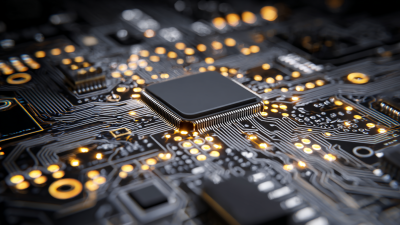
In the rapidly evolving world of printed circuit board (PCB) design, the significance of solder mask techniques cannot be overstated. According to a report by Electronics Design, the global PCB market is projected to reach $77.57 billion by 2029, driven by the increasing demand for electronic devices across various sectors. A well-applied solder mask not only enhances the aesthetic appeal of PCB designs but also plays a crucial role in protecting conductive pathways and preventing solder bridging during assembly. As the complexity of electronic circuits grows, mastering advanced solder mask techniques becomes essential for engineers and designers aiming to optimize PCB performance and reliability. This digital guide seeks to demystify the intricacies of solder mask application, offering insights and strategies for enhancing your PCB designs in an increasingly competitive landscape.
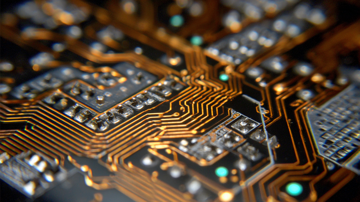
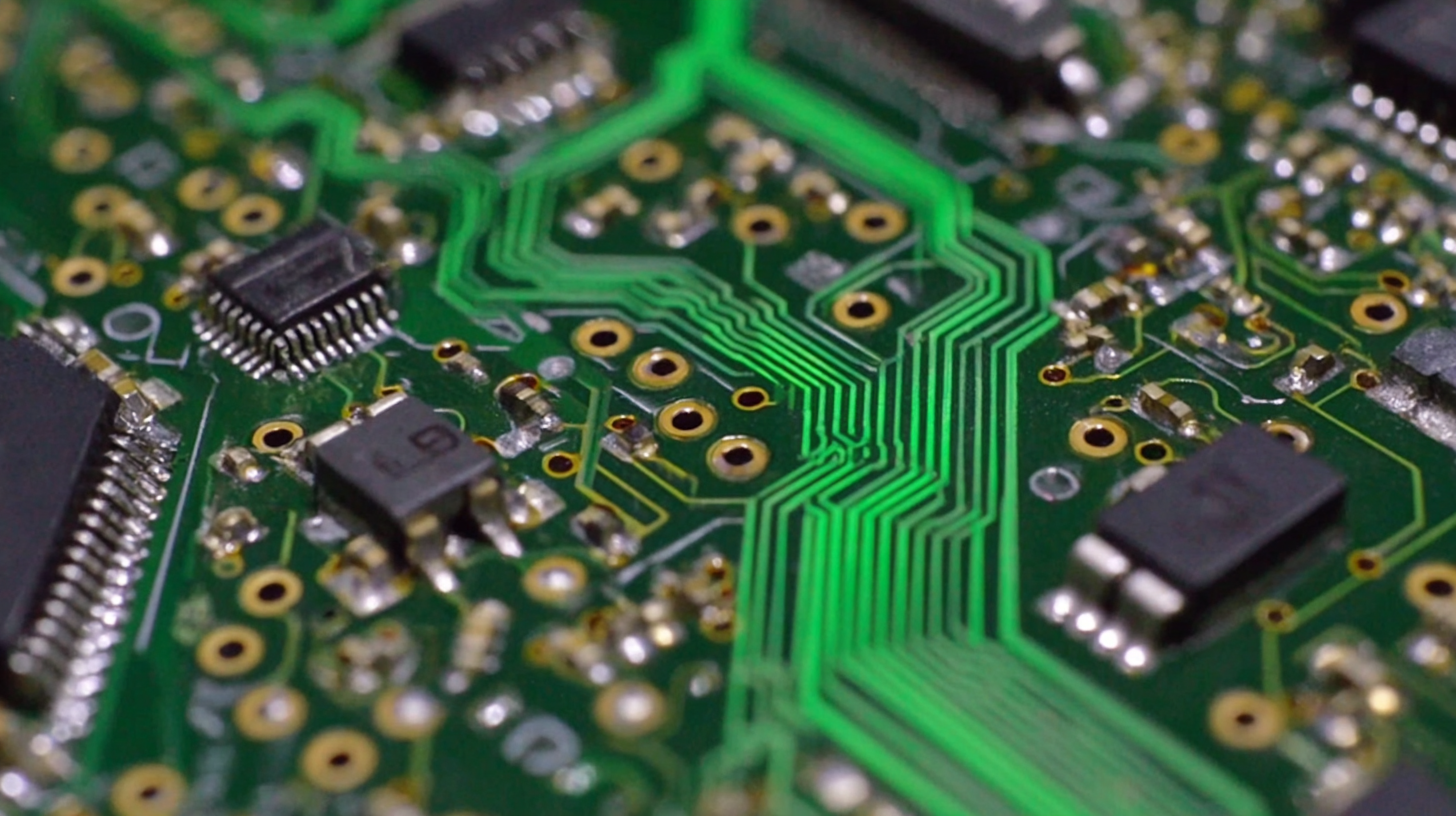
Solder mask plays a critical role in PCB design, acting as a protective layer that prevents solder from bridging conductive pathways. As electronics continue to trend towards miniaturization, the importance of effective solder mask techniques becomes even more pronounced. Modern challenges, such as working with ultra-fine pitch devices down to 0.3 mm, require precise solder mask application to ensure reliable performance and manufacturability. In fact, research indicates that a well-applied solder mask can improve the yield of complex designs by up to 30%.
When designing PCBs, selecting the right solder mask material is crucial. For instance, using a high-quality epoxy solder mask can enhance adhesion and provide better thermal stability, which is essential for today's high-density boards. Additionally, maintaining proper mask clearance around pads will help minimize solder balls and ensure better registration during the assembly process.
**Tips:**
1. Always account for thermal expansion differences between the solder mask and substrate materials to prevent delamination.
2. Consider implementing a verification process for solder mask alignment during production to enhance registration accuracy.
3. Regularly update your design practices based on the latest industry trends to stay ahead of challenges related to miniaturization and component density.
| Aspect | Importance | Common Techniques | Recommended Materials | Applications |
|---|---|---|---|---|
| Solder Mask Material | Prevents solder bridging and protects the copper. | Photoimageable, Epoxy-based, Liquid & Dry Film. | Acrylic, Polyimide. | Consumer electronics, Automotive PCBs. |
| Thickness Control | Affects solder adhesion and PCB mechanical properties. | Laser etching, Thermal curing. | Standardized solder mask thickness variances. | High-density interconnects, RF circuits. |
| Color Selection | Enhances aesthetics and functionality. | UV stable inks, Custom colors. | Black, Green, Blue, Red. | LED lighting, Custom PCB projects. |
| Surface Finish | Impacts solderability and assembly processes. | Electroplated, Hot air level, Immersion. | ENIG, OSP, HASL. | Telecommunications, Aerospace. |
| Environmental Considerations | Influences the sustainability of PCB manufacturing. | Lead-free solder mask options. | Eco-friendly materials. | Green technology products, Medical devices. |
When it comes to enhancing PCB designs, understanding the different types of solder mask materials and their specific applications is crucial. The market for solder masks has been steadily growing, with a report by MarketsandMarkets projecting an increase from $1.2 billion in 2020 to $1.8 billion by 2025, driven by the rising demand in automotive and consumer electronics. Solder masks can primarily be categorized into two types: epoxy and liquid photoimageable (LPI) masks. Epoxy masks offer excellent mechanical properties and chemical resistance, making them ideal for high-reliability applications. Meanwhile, LPI masks are favored for their fine-line capabilities, allowing for complex designs that require precise detailing.
When selecting solder mask materials, it’s essential to consider the PCB's intended use and environmental conditions. For instance, if the PCB is expected to undergo thermal cycling, choosing a high-temperature solder mask would be beneficial. Tips: Always ensure compatibility with the substrate and other materials used in your PCB. Additionally, applying a solder mask with a matte finish can help prevent solder bridging during assembly, leading to a more efficient production process. As you explore different solder mask options, conduct thorough testing to guarantee that the selected material meets or exceeds industry standards.
Solder mask application is a crucial step in PCB design, impacting both the performance and longevity of electronic devices. Effective techniques for applying solder mask can significantly enhance the reliability of solder joints and minimize the risk of solder bridging. According to industry reports, improper application of solder mask can lead to over 30% of production defects in PCBs. By utilizing techniques such as precise application methods like stencil printing and spray coating, manufacturers can ensure a uniform layer that adheres properly to the substrate, reducing the chances of failures.
Moreover, advancements in materials have allowed for the development of high-performance solder masks that improve thermal stability and chemical resistance. A 2022 study highlighted that PCBs utilizing advanced solder mask technologies showed a 50% decrease in thermal-related failures. This is particularly significant for high-performance applications, such as gaming laptops and other devices that demand efficient heat dissipation. As PCB technology continues to evolve, mastering solder mask application techniques will be essential for engineers seeking to push the boundaries of what their designs can achieve.
 Mastering solder mask techniques is crucial in the evolving landscape of PCB designs, especially with the rising complexity brought on by 5G technology. As these designs demand compactness and high power density, engineers often face challenges including alignment of multiple connectors and enhanced heat dissipation requirements. Addressing these challenges requires a strategic approach and an understanding of common solder mask applications.
One critical tip for overcoming these challenges is to communicate early with connector suppliers. Understanding their specifications can help avoid alignment issues that often occur during the PCB fabrication process. Additionally, designers should employ advanced thermal management techniques, such as incorporating thermal vias or using high-performance materials, to ensure adequate heat dissipation despite the small footprint of modern 5G components.
Moreover, optimizing solder mask application through proper thickness and alignment is essential. A well-applied solder mask can significantly reduce the risk of solder bridging, which is particularly important in high-density designs. Utilizing specialized manufacturing techniques, like screen printing or custom solder masks, can further enhance reliability and performance in today's fast-paced technological environment.
When it comes to designing printed circuit boards (PCBs), the importance of effective solder mask techniques cannot be overstated. A well-executed solder mask not only protects the PCB from environmental damage but also enhances the overall performance of the circuitry. Key best practices in designing solder masks can significantly improve yield rates and reduce manufacturing defects, ultimately leading to better product reliability.


„Thanks to the LUVIR technology, the solder resist process could be switched directly from the previously used mask exposure to direct exposure. As an outstanding digital solution on the market, this technology has been able to demonstrate fast process times and superior quality on our certified conventional ink in production. This allowed us to fully digitize the solder mask process at low cost – without process or ink adjustments. An excellent benefit to our production in Rot am See.“
Ralf Göhringer (Head of Production WE Rot am See)
I would definitely recommend the Limata machine and team for a future company purchase
Michael Greenaway
Compunetics Inc.
“The Limata ldi has been amazing!! Best thing we did was buy this machine”
Richard Brady
GM
Circuitlabs
“Since 2019, we have been running the Limata X1000 LDI system (including LUVIR for solder mask imaging) in daily production as an addition to our current process with film. The machine was capable of properly exposing Taiyo PSR-4000 BN (DI) solder mask types on normal to high-copper boards using a new and unique direct imaging process. The machine operating interface is very user friendly which allowed for a quick technical training curve. The pre-registration processing reduced several seconds of production time at every print. Limata support and service staff is incomparable. They supported our team every step of the way at basically any time of the day or night, with literally, an immediate response time, customizing the software interface to best fit our Operations and needs.
We have exposed more than 8,000 prints since end of October, on various solder mask colors and some resist film panels. Limata, has proven to be very capable and innovative. They are a strong contender in the industry.
We have very much enjoyed this project, and working with the team!
Thank you Limata for the continued support and being a part of our growth.”
Bill Sezate
Vice President, GM
Summit Interconnect
As a replacement to our current contact exposure process with film, the LIMATA X2000 system including LUVIR-Technology was capable of properly exposing non-LDI solder mask types using a direct imaging process. The machine offers cutting edge software with a very intuitive operating interface which allowed for quick technician training curve. The dual drawer system combined with pre-registration processing reduced several seconds of production time at every machine cycle. Limata support and service staff is world class. They added software patches to keep production running at shortest possible response times, customized the software interface to best fit our in-house Operations system, and even wrote a step-by-step machine processing manual. As a result of the project, we have exposed more than 16,000 times on various product types and solder mask brands/colors. Limata, in a very short timeframe as a company, has definitely shown they are truly innovative and will be challenging the industry of direct imaging for the top spot.
Kevin Beattie
Process Engineer
TTM Technologies
Forest Grove Division