The application of solder mask is a critical process in printed circuit board (PCB) manufacturing, directly impacting the performance and longevity of electronic devices. According to a 2022 IPC report, improper solder mask application can lead to increased failure rates of PCBs, with as much as 30% of failures attributed to issues in this phase. Solder mask not only protects against environmental factors and mechanical stress but also plays a vital role in enhancing the electrical performance by preventing solder bridging and minimizing oxidation.

With the global PCB market projected to reach $100 billion by 2025, optimizing solder mask application is essential for manufacturers aiming to meet the growing demands for reliability and efficiency in high-performance electronics. In this guide, we will explore effective strategies to enhance solder mask application, thereby boosting the overall quality and durability of PCBs in a competitive market landscape.
The solder mask plays a crucial role in the performance and reliability of printed circuit boards (PCBs). Serving as a protective layer, it safeguards the copper traces from environmental factors such as moisture, dust, and chemicals that can lead to corrosion and ultimately failure. By preventing solder from bridging between conductors, the solder mask enhances the integrity of electrical connections, reducing the risk of short circuits and improving overall reliability. This protective function is essential in applications where PCB longevity is critical, such as in aerospace and medical devices.
 Additionally, the quality and application of the solder mask can significantly affect the thermal and electrical performance of a PCB. A well-applied solder mask not only protects but also improves the thermal dissipation properties of the circuit, helping it to operate efficiently under varying temperatures. The choice of solder mask material, thickness, and the precision of its application can influence the board's mechanical strength and resistance to delamination. By understanding these factors and optimizing the solder mask application process, manufacturers can enhance both the performance and lifespan of PCBs, ensuring they meet the ever-increasing demands of modern electronic devices.
When it comes to PCB (Printed Circuit Board) design, the choice of solder mask significantly influences thermal management and overall performance. Solder masks come in various types—epoxy, liquid photoimageable (LPI), and dry film—each offering distinct characteristics. For instance, epoxy-based solder masks are known for their excellent thermal resistance, making them suitable for high-temperature applications. In contrast, LPI solder masks provide superior coverage and finer line definition, beneficial for intricate circuit layouts and efficient heat dissipation.
**Tips: Use the Right Solder Mask for Your Application**
Selecting the correct solder mask type based on the application can prevent overheating and extend PCB lifespan. For areas of the board that experience high thermal loads, consider using materials specifically designed for heat resistance. Additionally, applying solder masks in a thin layer can enhance heat transfer, as excess material can act as an insulator rather than a conductor.
Another essential consideration is the solder mask's ability to withstand environmental factors. A robust solder mask can protect PCBs from moisture and contaminants, which can degrade performance over time. Testing different solder mask options during the prototyping phase helps in identifying the optimal type for managing heat and ensuring long-lasting performance.
| Solder Mask Type | Thermal Conductivity (W/m·K) | Dielectric Constant | Tensile Strength (MPa) | Impact on PCB Longevity |
|---|---|---|---|---|
| Epoxy-Based Solder Mask | 0.2 | 3.5 | 60 | Good |
| Polyimide Solder Mask | 0.25 | 3.0 | 90 | Excellent |
| Liquid Photoimageable Solder Mask | 0.15 | 3.2 | 50 | Moderate |
| Green Solder Mask (Traditional) | 0.1 | 3.8 | 45 | Fair |
| Hasl (Hot Air Solder Leveling) | 0.18 | 3.6 | 55 | Good |
When it comes to PCB manufacturing, the application of solder mask plays a crucial role in enhancing performance and longevity. Best practices in solder mask application begin with meticulous surface preparation. This step involves cleaning the PCB substrate thoroughly to remove any contaminants that could compromise adhesion. Techniques such as rinsing with a suitable solvent and employing a plasma treatment can significantly improve the bonding of the solder mask, ensuring a uniform application that reduces defects.
Another vital aspect is the selection of the right solder mask material. Depending on the specific requirements of the PCB, manufacturers can choose between various types of solder masks, such as epoxy or liquid photoimageable (LPI) masks. Each type has its advantages: while epoxy masks offer excellent durability, LPI masks provide finer detail and better precision. The application process should also be closely monitored; using appropriate curing techniques and controlling the temperature and humidity can lead to optimal results. Alongside these practices, consistent quality checks throughout the application process ensure adhesion strength and overall performance, ultimately contributing to the longevity of the PCB.
This chart illustrates the impact of various solder mask application parameters on PCB performance. The data highlights key metrics such as adhesion strength, surface smoothness, drying time, and thickness, all of which play a critical role in ensuring the longevity and reliability of printed circuit boards.
Proper solder mask curing is essential for maximizing the lifespan of printed circuit boards (PCBs). When the solder mask is cured accurately, it creates a robust barrier that protects the copper traces and prevents oxidation and corrosion, which are common threats to PCB integrity over time. Quantifying the benefits of this process reveals not only improved durability but also enhanced performance under various operating conditions.

Furthermore, the curing process can significantly affect the thermal properties of the solder mask. A well-cured solder mask can withstand higher temperatures without degrading, reducing the risk of failure in high-temperature environments. This resilience can lead to fewer repairs and replacements over the lifecycle of the PCB, thereby lowering overall costs. Regular assessments of solder mask applications, along with precise curing methods, can yield tangible benefits in both the reliability and efficiency of electronic devices.
The thickness of solder mask plays a critical role in determining the signal integrity of printed circuit boards (PCBs). A thicker solder mask can serve to shield trace routes more effectively, minimizing the crosstalk and interference that can occur between closely packed circuits. When the solder mask is applied uniformly, it helps maintain a consistent dielectric layer, which is essential for high-frequency signals. Variations in thickness can introduce impedance mismatches that lead to signal degradation, affecting the performance of the PCB, especially in high-speed and high-frequency environments.
Moreover, solder mask thickness directly influences electromagnetic interference (EMI) mitigation. A well-optimized solder mask can act as a barrier against external electromagnetic fields, helping to protect sensitive components on the PCB from interference. By selecting an appropriate thickness for the solder mask, designers can enhance the board's overall reliability, ensuring that it meets stringent compliance standards while maintaining operational integrity in a variety of environments. Thus, careful consideration of solder mask thickness during the design phase can lead to improved performance and longevity of electronic devices.
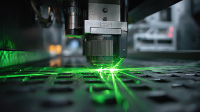

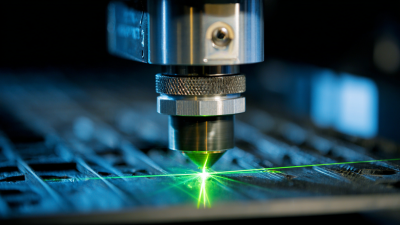

„Thanks to the LUVIR technology, the solder resist process could be switched directly from the previously used mask exposure to direct exposure. As an outstanding digital solution on the market, this technology has been able to demonstrate fast process times and superior quality on our certified conventional ink in production. This allowed us to fully digitize the solder mask process at low cost – without process or ink adjustments. An excellent benefit to our production in Rot am See.“
Ralf Göhringer (Head of Production WE Rot am See)
I would definitely recommend the Limata machine and team for a future company purchase
Michael Greenaway
Compunetics Inc.
“The Limata ldi has been amazing!! Best thing we did was buy this machine”
Richard Brady
GM
Circuitlabs
“Since 2019, we have been running the Limata X1000 LDI system (including LUVIR for solder mask imaging) in daily production as an addition to our current process with film. The machine was capable of properly exposing Taiyo PSR-4000 BN (DI) solder mask types on normal to high-copper boards using a new and unique direct imaging process. The machine operating interface is very user friendly which allowed for a quick technical training curve. The pre-registration processing reduced several seconds of production time at every print. Limata support and service staff is incomparable. They supported our team every step of the way at basically any time of the day or night, with literally, an immediate response time, customizing the software interface to best fit our Operations and needs.
We have exposed more than 8,000 prints since end of October, on various solder mask colors and some resist film panels. Limata, has proven to be very capable and innovative. They are a strong contender in the industry.
We have very much enjoyed this project, and working with the team!
Thank you Limata for the continued support and being a part of our growth.”
Bill Sezate
Vice President, GM
Summit Interconnect
As a replacement to our current contact exposure process with film, the LIMATA X2000 system including LUVIR-Technology was capable of properly exposing non-LDI solder mask types using a direct imaging process. The machine offers cutting edge software with a very intuitive operating interface which allowed for quick technician training curve. The dual drawer system combined with pre-registration processing reduced several seconds of production time at every machine cycle. Limata support and service staff is world class. They added software patches to keep production running at shortest possible response times, customized the software interface to best fit our in-house Operations system, and even wrote a step-by-step machine processing manual. As a result of the project, we have exposed more than 16,000 times on various product types and solder mask brands/colors. Limata, in a very short timeframe as a company, has definitely shown they are truly innovative and will be challenging the industry of direct imaging for the top spot.
Kevin Beattie
Process Engineer
TTM Technologies
Forest Grove Division