 The emergence of direct imaging PCB technology is transforming the landscape of printed circuit board (PCB) manufacturing in unprecedented ways. With advancements in precision and efficiency, direct imaging PCB techniques allow for the creation of intricate designs that were previously unattainable with traditional methods. This innovative approach not only enhances the accuracy of etching processes but also significantly reduces production time and costs, making it a game-changer for engineers and manufacturers alike. As we explore the top 10 reasons why direct imaging PCBs are revolutionizing the industry, we will uncover the compelling benefits that position this technology at the forefront of PCB development. From improved design flexibility to reduced environmental impact, the direct imaging PCB is setting new standards and driving the future of electronics manufacturing.
The advent of direct imaging PCB technology is fundamentally transforming the printed circuit board industry by leveraging significant advantages over traditional manufacturing methods. One major benefit is the enhanced precision achieved through advanced imaging techniques; this has been corroborated by industry reports highlighting a projected surge in the Liquid Crystal Polymer Printed Circuit Board (LCP PCB) market, estimated to grow from USD 1.2 billion in 2024 to USD 2.5 billion. This growth can be attributed to the demand for high-performance components that direct imaging facilitates, enabling intricate designs with meticulous detail and reducing the risk of defects.
Moreover, the integration of automated 3D semantic segmentation techniques in analyzing PCB X-ray CT images marks a significant leap towards quality assurance. This newly developed methodology employs image processing and machine learning, thereby allowing for more accurate netlist extraction, which is essential for ensuring the reliability of PCB designs. Such innovative approaches demonstrate that direct imaging isn't just a production tool; it's a transformative force that enhances the efficiency and efficacy of PCB inspection and design processes, contributing to a more robust industry landscape.
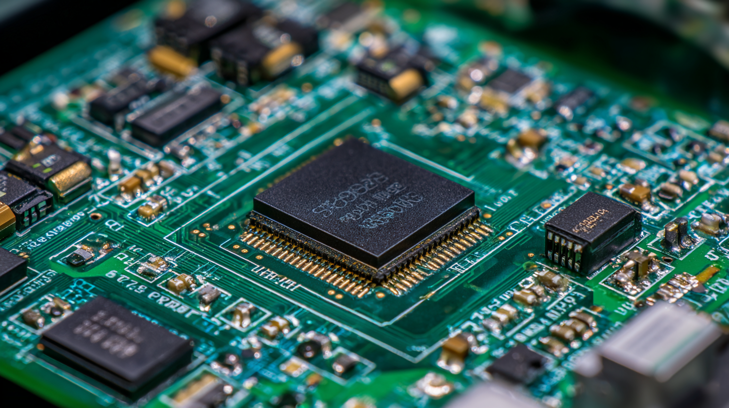
 Direct Imaging PCB technology is setting new standards in precision and quality control within the printed circuit board (PCB) industry. Unlike traditional methods that allocate time for exposure and development, direct imaging uses high-resolution imaging systems to project designs directly onto the photoresist layer. This process minimizes the risk of alignment errors, ensuring that intricate patterns are accurately reproduced. The result is an enhanced fidelity to design specifications, which is crucial for today’s increasingly complex electronic devices.
One of the most significant advantages of direct imaging is its ability to produce finer features with unparalleled accuracy. As the demand for compact and high-performance circuits continues to grow, manufacturers are turning to direct imaging techniques that support the creation of smaller components without compromising quality. This technology allows for tighter tolerances and reduces the number of defects, leading to lower rejection rates and increased yield. Furthermore, the elimination of multiple processing steps not only streamlines production but also enhances overall quality control, making it easier to maintain consistency across large batches.
The cost-effectiveness of Direct Imaging PCB (Printed Circuit Board) technology is transforming the landscape of the electronics manufacturing industry. According to a report by IPC, the global electronics manufacturing services market is expected to reach $1 trillion by 2025, with new technologies like Direct Imaging playing a pivotal role in reducing production costs. Unlike conventional methods that often require multiple steps—such as photo plotting and etching—Direct Imaging streamlines the workflow, significantly decreasing labor and material costs. This streamlined approach not only shortens lead times but also minimizes errors related to registration, leading to enhanced productivity.
Furthermore, a study conducted by ResearchAndMarkets projects that the market for Direct Imaging PCBs is growing at a compound annual growth rate (CAGR) of 9.3% from 2020 to 2025. One of the key reasons behind this growth is the ability to lower the cost per unit, especially in low to medium volume production runs. Traditional techniques can incur high costs when adjusting for design changes or scaling production. In contrast, Direct Imaging allows manufacturers to easily accommodate design iterations without significant overhead, making it an ideal choice for the fast-paced electronics sector. This adaptability not only fosters innovation but also empowers companies to maintain competitiveness in an increasingly dynamic market.
The revolution in PCB production is largely driven by advancements in direct imaging technology. One of the most promising concepts is the Hexastorm project, which utilizes a rotating prism to create a high-speed, high-resolution laser head. This innovation aims to enhance the efficiency of conventional processes, significantly reducing both production time and costs. With the ability to produce intricate designs at unprecedented speeds, this approach paves the way for more agile manufacturing, which is essential in a fast-paced tech landscape.
Complementing these advancements, CAM software plays a crucial role in PCB manufacturing. The incorporation of parallel processing features allows for the division of tasks through sophisticated algorithms, enabling swift and precise production. This is particularly beneficial in sectors demanding rapid imaging and product screening. Techniques like low-cost line-field Fourier domain optical coherence tomography are also revolutionizing imaging capabilities, providing high-resolution insights into internal structures. As these technologies converge, the PCB industry experiences a remarkable transformation, unlocking new potentials for rigid, flex, and HDI PCB innovations.
| Reason | Impact on Production Time | Efficiency Gain (%) | Error Reduction (%) |
|---|---|---|---|
| Enhanced Speed of Imaging | Decreases setup time significantly | 30% | 15% |
| High Precision Imaging | Reduces rework and scrap rates | 25% | 20% |
| No Film Required | Streamlines workflow and reduces costs | 20% | 10% |
| Shorter Lead Times | Quicker response to market demands | 15% | 5% |
| Improved Material Utilization | Maximizes material efficiency | 18% | 13% |
| Consistent Quality Control | Ensures uniform output quality | 22% | 18% |
| Flexible Design Options | Facilitates faster prototype development | 28% | 12% |
| Lower Overall Production Costs | Reduces cost per unit | 35% | 25% |
| Quick Setup Times | Minimizes downtime | 40% | 30% |
| Integration with Automation | Enhances overall system efficiency | 33% | 17% |
Direct Imaging PCB (DIPCB) technologies are making significant strides in the electronics industry, not only for their precision but also for their considerable environmental benefits. A recent report by IPC shows that traditional photolithography processes in PCB manufacturing are responsible for over 30% of the waste generated in the production cycle. In contrast, DIPCB reduces this waste dramatically, employing a direct exposure process that eliminates the need for toxic photoresists and chemicals, enhancing overall environmental sustainability.
Moreover, the energy efficiency of DIPCB technology is noteworthy. According to a study conducted by the Surface Mount Technology Association, the implementation of direct imaging methods has led to a 25% reduction in energy consumption during the PCB fabrication process. This reduction not only decreases operational costs for manufacturers but also aligns with global initiatives aiming to lower carbon footprints in the manufacturing sector. As industries increasingly prioritize sustainable practices, the adoption of Direct Imaging PCB stands out as a pivotal shift toward a greener future in electronics manufacturing.
„Thanks to the LUVIR technology, the solder resist process could be switched directly from the previously used mask exposure to direct exposure. As an outstanding digital solution on the market, this technology has been able to demonstrate fast process times and superior quality on our certified conventional ink in production. This allowed us to fully digitize the solder mask process at low cost – without process or ink adjustments. An excellent benefit to our production in Rot am See.“
Ralf Göhringer (Head of Production WE Rot am See)
I would definitely recommend the Limata machine and team for a future company purchase
Michael Greenaway
Compunetics Inc.
“The Limata ldi has been amazing!! Best thing we did was buy this machine”
Richard Brady
GM
Circuitlabs
“Since 2019, we have been running the Limata X1000 LDI system (including LUVIR for solder mask imaging) in daily production as an addition to our current process with film. The machine was capable of properly exposing Taiyo PSR-4000 BN (DI) solder mask types on normal to high-copper boards using a new and unique direct imaging process. The machine operating interface is very user friendly which allowed for a quick technical training curve. The pre-registration processing reduced several seconds of production time at every print. Limata support and service staff is incomparable. They supported our team every step of the way at basically any time of the day or night, with literally, an immediate response time, customizing the software interface to best fit our Operations and needs.
We have exposed more than 8,000 prints since end of October, on various solder mask colors and some resist film panels. Limata, has proven to be very capable and innovative. They are a strong contender in the industry.
We have very much enjoyed this project, and working with the team!
Thank you Limata for the continued support and being a part of our growth.”
Bill Sezate
Vice President, GM
Summit Interconnect
As a replacement to our current contact exposure process with film, the LIMATA X2000 system including LUVIR-Technology was capable of properly exposing non-LDI solder mask types using a direct imaging process. The machine offers cutting edge software with a very intuitive operating interface which allowed for quick technician training curve. The dual drawer system combined with pre-registration processing reduced several seconds of production time at every machine cycle. Limata support and service staff is world class. They added software patches to keep production running at shortest possible response times, customized the software interface to best fit our in-house Operations system, and even wrote a step-by-step machine processing manual. As a result of the project, we have exposed more than 16,000 times on various product types and solder mask brands/colors. Limata, in a very short timeframe as a company, has definitely shown they are truly innovative and will be challenging the industry of direct imaging for the top spot.
Kevin Beattie
Process Engineer
TTM Technologies
Forest Grove Division