Printed circuit boards rarely fail in dramatic ways. A microscopic copper break, a solder bridge, or a weak plated-through hole can quietly interrupt a signal. Electrical Testing Pcb methods help uncover these defects before boards reach assembly or service. The need is growing with the market: Grand View Research’s Printed Circuit Board Market Size, Share & Trends Analysis Report estimated the global PCB market at USD 76.2 billion in 2023. More production means more value in verifying every connection.
The main methods answer different questions. Continuity and isolation tests check whether intended paths conduct and unwanted paths remain separate. A bed-of-nails fixture tests many points quickly, making it useful for repeat production. Flying-probe testing uses movable probes and avoids a dedicated fixture, which can suit prototypes and low-volume runs. Boundary-scan testing checks access through compatible chips, while functional testing evaluates a board’s behavior under defined operating conditions. Each method has limits. No test catches everything.
IPC-9252B, Requirements for Electrical Testing of Unpopulated Printed Boards, provides industry guidance for bare-board testing. IPC’s 2023 North American PCB Production report adds manufacturing context, where product mix and production scale shape inspection choices. In practice, engineers often combine methods: a flying probe for early revisions, then fixture-based testing as volume rises. The right choice depends on access, pitch, cost, and risk—not a single “best” machine. Test plans also need review; a clean pass can still miss faults outside the test’s coverage.
Continuity testing checks whether each intended PCB path remains electrically connected from pad to pad, via to via, or connector to component. A flying-probe tester touches exposed points and compares measured resistance with the board’s specified limits. IPC-9252B, the industry specification for electrical testing of unpopulated printed boards, addresses continuity and isolation checks. Limits should match the design: a long, narrow copper trace will not read like a short, wide power plane. Small differences matter.
Short-circuit testing looks for unintended connections between separate nets, often caused by solder bridges, copper slivers, or damaged insulation. Test software compares the measured netlist against the board’s design data, then flags unexpected low-resistance paths. For example, an engineer might check all 800 nets on a sample board and investigate any unexpected connection between adjacent fine-pitch pads. That figure is illustrative, not an industry-wide benchmark. IPC-6012 provides additional performance and qualification requirements for rigid boards, while the actual acceptance thresholds depend on the drawing and customer specification. Keep the fixture clean, confirm probe contact, and retest suspicious readings; a little contamination can imitate a fault. I have seen teams trust one test pass too quickly. That can be a costly assumption.
Continuity and short-circuit testing check that intended connections have low resistance and that isolated nets remain electrically separated.
How to read it: Continuity readings should be low; resistance between isolated nets should be high. The values shown are illustrative examples, not test results or universal pass limits. Acceptable thresholds depend on the PCB design, test method, and applicable requirements.
Insulation resistance testing checks whether adjacent PCB conductors remain electrically isolated. A small residue of flux, moisture, or dust can create a leakage path between fine-pitch traces. The test applies a controlled voltage between conductors and measures resistance, usually in megaohms. Tiny gaps matter. IPC-9202A, the Surface Insulation Resistance Handbook, and IPC-TM-650 Method 2.6.3.7 describe established approaches for evaluating surface insulation under controlled conditions. A commonly used screening benchmark is 100 megohms, but the acceptance limit depends on the product specification and test setup.
For a meaningful result, engineers record conductor spacing, test voltage, temperature, humidity, and exposure time. A clean, dry board may pass quickly, while humidity can reveal leakage that ordinary continuity checks miss. This is why qualification testing often uses elevated humidity and electrical bias over an extended period. Compare readings before and after conditioning, not just one final number. Still, a high resistance reading does not prove every board will remain reliable in service. Test coupons may not reproduce every narrow gap, contamination spot, or assembly condition. That limitation deserves attention when selecting coupon locations and setting acceptance criteria.
| Test Dimension | What Is Evaluated | Typical Practice | Result or Interpretation |
|---|---|---|---|
| Test objective | Electrical leakage between PCB conductors that are intended to remain isolated. | Apply a DC voltage between selected nets, traces, or conductors and measure the resulting leakage current. | Lower leakage generally corresponds to higher insulation resistance. |
| Measurement principle | Resistance between the energized conductor and the conductor held at the reference potential. | Calculate resistance using R = V ÷ I, where voltage is in volts and current is in amperes. | Results are commonly expressed in megohms (MΩ) or gigohms (GΩ). |
| Test voltage | The DC potential used to assess insulation between the selected conductors. | Choose the voltage from the applicable product specification and test procedure. Instrument settings such as 100 V, 250 V, or 500 V DC may be used when appropriate. | There is no single voltage suitable for every PCB. The selected level must not exceed the limits of the board, components, or test specification. |
| Measurement interval | Insulation resistance after the test voltage has been applied for a defined period. | Use the dwell time specified by the governing procedure; record the interval because readings can change as the insulation responds to applied voltage. | Compare readings only when voltage, dwell time, and environmental conditions are defined consistently. |
| Test equipment | Small leakage currents and the corresponding high resistance values. | Use a calibrated insulation-resistance meter or suitable high-resistance measurement instrument, with appropriate fixtures and safe handling procedures. | Instrument range, calibration status, fixture leakage, and connection quality can affect the reading. |
| Conductors under test | Specific pairs of electrically isolated conductors, such as adjacent nets or conductors separated by PCB dielectric. | Identify the test points and confirm that connected circuitry will not create unintended current paths. | For populated boards, components and circuit paths may affect the measurement; test connections must account for the board design. |
| Environmental influences | Changes in insulation resistance associated with board condition and test environment. | Keep the board clean and dry, and record relevant temperature and humidity conditions when the test procedure requires them. | Moisture, ionic contamination, and surface residues can increase leakage and reduce measured resistance. |
| Acceptance criteria | Whether the measured insulation resistance meets the required product or process limit. | Set the pass/fail threshold in the applicable design, customer, or test specification, together with the voltage and measurement interval. | A universal minimum resistance value should not be assumed; acceptance limits depend on the applicable requirements and test conditions. |
Note: Insulation-resistance testing is distinct from a dielectric-withstand test. Use the voltage, duration, connections, and acceptance criteria specified for the PCB and its intended application.
Dielectric withstand testing checks whether a PCB’s insulation can resist a specified voltage without breaking down. A test voltage is applied between electrically isolated points, such as primary circuits and accessible conductive parts. The tester monitors leakage current during a controlled test period. Any flashover, breakdown, or current above the permitted limit may indicate an insulation weakness.
Details matter. Test voltage, ramp rate, and duration should match the product requirements and applicable standards. Applying excessive voltage can damage components or weaken insulation, so the test setup should isolate sensitive circuits where required. Before testing, technicians typically inspect the board for contamination, solder debris, and damaged coating. A tiny metal fragment can change the result.
A passing test is useful evidence, not a guarantee of lifetime reliability. It may not reveal every defect, especially when moisture, heat, or vibration later affect the board. That limitation deserves attention. Keep test records, verify equipment calibration, and investigate unexpected leakage rather than simply repeating the test. Clear procedures make results more repeatable, though real production conditions are rarely perfect.
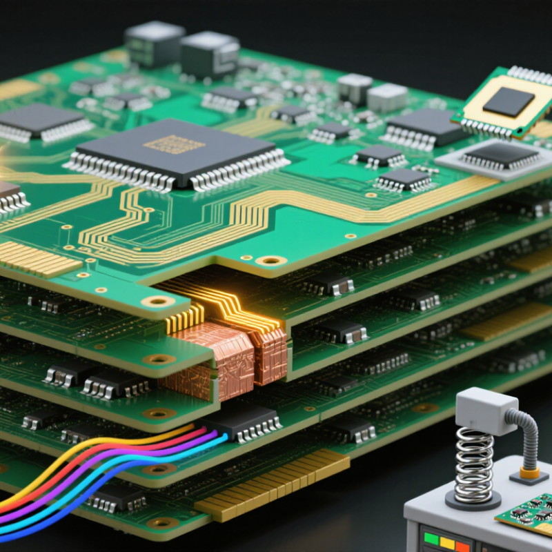
In-circuit testing (ICT) checks electrical connections and selected component values on an assembled PCB. A bed-of-nails fixture uses spring-loaded pins to contact many test points at once. This makes it useful for repeat production, where rapid, consistent checks matter. Contact matters. Poorly supported boards or dirty pins can cause intermittent readings, so fixture condition and board support need regular attention. The fixture is designed for a particular board layout, which can add cost and limit flexibility when test points change.
Flying-probe systems move a small number of probes across the board, avoiding a dedicated fixture. They can suit prototypes, small production runs, and designs that change often, though testing usually takes longer. Probe access still depends on suitable exposed pads and spacing. Not always. Dense layouts may leave important nodes unreachable. ICT can reveal opens, shorts, and certain assembly faults, but it does not confirm that the PCB performs correctly in its final application. Component interactions can also make readings difficult to interpret. A practical test plan balances coverage, production volume, access, and the consequences of a missed fault; engineers should review borderline results against the schematic and known-good measurements.
Functional testing checks whether an assembled PCB performs its intended tasks while powered, not merely whether its traces connect. Engineers apply the specified supply voltage, load, input signals, and communication traffic, then record outputs, current draw, timing, and fault flags. A temperature-controlled chamber can reveal intermittent behavior as components warm. Watch the readings closely.
For qualification, JEDEC JESD22-A104F defines temperature-cycling test conditions, including profiles spanning −55°C to +125°C; this is a stress-test range, not a universal operating specification. IPC-9701A describes methods for evaluating surface-mount solder-attachment reliability, including monitoring electrical continuity during cycling. These standards help teams choose repeatable conditions and track failures over time. On the production line, functional limits should still come from the product’s documented operating range. A board that passes at room temperature may fail when a connector carries full load or a processor changes state. That gap is easy to miss. Test plans also need clear limits for acceptable voltage, response time, and current. One imperfect area is fixture coverage: test points cannot reproduce every real-world cable, enclosure, or thermal path. Record that limitation, review failure logs, and update the test when field evidence exposes a blind spot.
„Thanks to the LUVIR technology, the solder resist process could be switched directly from the previously used mask exposure to direct exposure. As an outstanding digital solution on the market, this technology has been able to demonstrate fast process times and superior quality on our certified conventional ink in production. This allowed us to fully digitize the solder mask process at low cost – without process or ink adjustments. An excellent benefit to our production in Rot am See.“
Ralf Göhringer (Head of Production WE Rot am See)
I would definitely recommend the Limata machine and team for a future company purchase
Michael Greenaway
Compunetics Inc.
“The Limata ldi has been amazing!! Best thing we did was buy this machine”
Richard Brady
GM
Circuitlabs
“Since 2019, we have been running the Limata X1000 LDI system (including LUVIR for solder mask imaging) in daily production as an addition to our current process with film. The machine was capable of properly exposing Taiyo PSR-4000 BN (DI) solder mask types on normal to high-copper boards using a new and unique direct imaging process. The machine operating interface is very user friendly which allowed for a quick technical training curve. The pre-registration processing reduced several seconds of production time at every print. Limata support and service staff is incomparable. They supported our team every step of the way at basically any time of the day or night, with literally, an immediate response time, customizing the software interface to best fit our Operations and needs.
We have exposed more than 8,000 prints since end of October, on various solder mask colors and some resist film panels. Limata, has proven to be very capable and innovative. They are a strong contender in the industry.
We have very much enjoyed this project, and working with the team!
Thank you Limata for the continued support and being a part of our growth.”
Bill Sezate
Vice President, GM
Summit Interconnect
As a replacement to our current contact exposure process with film, the LIMATA X2000 system including LUVIR-Technology was capable of properly exposing non-LDI solder mask types using a direct imaging process. The machine offers cutting edge software with a very intuitive operating interface which allowed for quick technician training curve. The dual drawer system combined with pre-registration processing reduced several seconds of production time at every machine cycle. Limata support and service staff is world class. They added software patches to keep production running at shortest possible response times, customized the software interface to best fit our in-house Operations system, and even wrote a step-by-step machine processing manual. As a result of the project, we have exposed more than 16,000 times on various product types and solder mask brands/colors. Limata, in a very short timeframe as a company, has definitely shown they are truly innovative and will be challenging the industry of direct imaging for the top spot.
Kevin Beattie
Process Engineer
TTM Technologies
Forest Grove Division