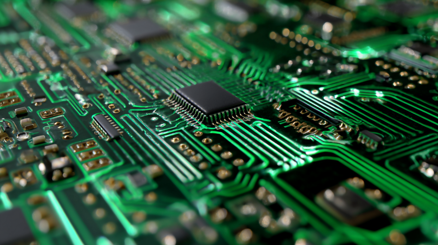
In the rapidly evolving landscape of electronics, mastering PCB technology is crucial for engineers and designers striving to deliver innovative and efficient products. According to a recent report by Markets and Markets, the global PCB market is projected to reach $87.5 billion by 2025, driven by the rising demand for consumer electronics and telecommunications. However, with advancements in technology come inherent challenges, such as design complexities, increasing miniaturization, and the need for higher reliability. This guide aims to address common problems associated with PCB technology, providing insights and solutions that will empower you to navigate these challenges in your projects effectively. Understanding the intricacies of PCB manufacturing and layout is essential in staying competitive in this dynamic field.

Advanced PCB technologies have a profound impact on modern electronics manufacturing, driving innovation and enhancing the performance of electronic devices. As consumer demand for more complex and compact gadgets increases, manufacturers are turning to cutting-edge PCB technologies like HDI (High-Density Interconnect) and flexible PCBs. These advancements allow for more intricate circuit designs, improved signal integrity, and greater heat dissipation, which are essential for the latest applications, from smartphones to IoT devices.
Moreover, the integration of advanced materials, such as embedded components and advanced laminates, further elevates PCB functionality. This not only helps in reducing the size of devices but also increases their reliability and efficiency. The adoption of automated manufacturing processes facilitated by these technologies minimizes human error and accelerates production timelines. As a result, companies can meet stringent market demands while maintaining high quality standards. The exploration of these technologies not only positions manufacturers at the forefront of the industry but also plays a critical role in shaping the future landscape of electronics.
The demand for high-quality printed circuit boards (PCBs) is surging, with the global market projected to grow by USD 26.8 billion from 2025 to 2029. This growth is primarily fueled by the rising adoption of smartphones and the increasing integration of artificial intelligence (AI) in PCB manufacturing processes. As these technologies evolve, understanding the key metrics driving market demand is crucial for professionals involved in PCB design and production.
To stay ahead in this competitive landscape, consider investing in education related to PCB technology. There are various online and offline courses available, from beginner to advanced levels, that can help you master the essential skills needed for successful projects. Engaging in these learning opportunities not only expands your technical knowledge but also enhances your ability to meet the market's increasing quality expectations.
Tip: When selecting a PCB supplier, focus on their manufacturing capabilities and quality assurance practices. A supplier that employs advanced techniques and testing protocols will likely deliver superior products. Additionally, keep an eye on industry trends and AI developments, as these innovations can significantly influence PCB functionality and performance. This proactive approach will position you well in the fast-evolving PCB market.
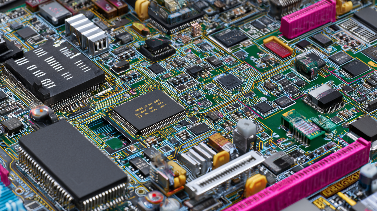
In the rapidly evolving field of electronics, selecting the right PCB manufacturer can significantly impact the success of your projects. A comparative analysis of leading PCB manufacturers reveals critical differences in production capabilities, technology used, and turnaround times. According to a 2022 industry report by IPC, nearly 50% of PCB manufacturers are expanding their production capacities to keep pace with increasing demand, particularly in sectors like automotive and telecommunications. This suggests that choosing a manufacturer with robust capabilities is essential for ensuring quality and reliability in your final products.
When evaluating PCB manufacturers, it's crucial to consider their technological advancements. For instance, companies utilizing advanced materials such as high-frequency substrates and thick copper layers can offer superior signal integrity for high-speed applications. Tip: Look for manufacturers that provide detailed specifications and certifications, such as UL approval, to ensure that they can meet the specific requirements of your project.
Additionally, turnaround time is a vital factor in your decision-making process. A timely production cycle can be the difference between meeting deadlines or delayed product launches. According to the same IPC report, manufacturers that invest in automation experience a 30% reduction in production time. Tip: Always inquire about the expected lead times during initial discussions with manufacturers to avoid surprises later in the development cycle.
This chart provides a comparative analysis of different PCB manufacturers based on their production capabilities, lead time, cost per unit, and quality rating. This information can help you decide which manufacturer best suits your project needs.
Emerging trends in PCB design are essential for understanding how innovations are shaping the future of electronics. According to a recent report by Mordor Intelligence, the global PCB market is expected to reach $100 billion by 2026, driven by rising demand in consumer electronics and the automotive industry. This growth underscores the importance of adopting advanced technologies such as multi-layer PCBs, which allow for more compact designs and greater functionality without increasing size—a crucial factor for modern devices.
Additionally, the integration of AI and machine learning into PCB design processes is revolutionizing the industry. Tools that utilize these technologies can predict design flaws and streamline production, resulting in a 25% reduction in time-to-market as noted in a study by IPC. As companies increasingly adopt these intelligent automation solutions, they gain the ability to innovate rapidly, reduce costs, and enhance product quality. The future of PCB design is not just about meeting current demands but anticipating the needs of a rapidly changing technological landscape.
| Trend | Description | Impact on Design | Future Outlook |
|---|---|---|---|
| Flexible PCBs | PCBs that can bend and flex, enabling new applications in wearable devices. | Allows for more compact designs and integration into small spaces. | Expected to grow with increased demand for wearable technology. |
| High-Frequency PCBs | Designed to operate at microwave frequencies, reducing signal loss. | Improves performance in telecommunications and radar technologies. | Increasing utilization in 5G technology and beyond. |
| Embedded Components | Components embedded within the PCB layers to save space. | Reduces footprint and enhances performance in high-density designs. | Projected to rise as miniaturization of devices continues. |
| Automated Design Tools | Software tools utilizing AI for automatic PCB layout and design optimization. | Accelerates the design process and minimizes human error. | Expected to become standard tools in PCB design workflows. |
| Sustainable PCB Manufacturing | Focus on reducing waste and using eco-friendly materials in PCB production. | Addresses environmental concerns and enhances compliance with regulations. | Growing trend as industries move towards greener practices. |
Quality assurance is a critical component in the production of printed circuit boards (PCBs), particularly as the demand for high-performance electronics continues to rise. To ensure compliance with international standards, manufacturers must implement well-defined metrics that evaluate each stage of the PCB production process. These metrics not only facilitate better quality control but also contribute to lean manufacturing principles by eliminating waste and enhancing overall efficiency.
Recent advancements in lean manufacturing have demonstrated the importance of integrating quality assurance into every aspect of production. By adopting methodologies that focus on continuous improvement, manufacturers can optimize their processes, reduce defects, and increase customer satisfaction. Implementing metrics such as defect rates, yield percentages, and cycle time can provide manufacturers with critical insights into their operations, leading to more informed decision-making and improved compliance with international standards.
As the technology driving PCB design and manufacturing evolves, so too must the quality assurance practices within the industry. Emphasizing the adoption of modern metrics aligned with international standards will empower manufacturers to not only meet but exceed customer expectations, ensuring the delivery of superior products while fostering a culture of quality and efficiency throughout their operations.
„Thanks to the LUVIR technology, the solder resist process could be switched directly from the previously used mask exposure to direct exposure. As an outstanding digital solution on the market, this technology has been able to demonstrate fast process times and superior quality on our certified conventional ink in production. This allowed us to fully digitize the solder mask process at low cost – without process or ink adjustments. An excellent benefit to our production in Rot am See.“
Ralf Göhringer (Head of Production WE Rot am See)
I would definitely recommend the Limata machine and team for a future company purchase
Michael Greenaway
Compunetics Inc.
“The Limata ldi has been amazing!! Best thing we did was buy this machine”
Richard Brady
GM
Circuitlabs
“Since 2019, we have been running the Limata X1000 LDI system (including LUVIR for solder mask imaging) in daily production as an addition to our current process with film. The machine was capable of properly exposing Taiyo PSR-4000 BN (DI) solder mask types on normal to high-copper boards using a new and unique direct imaging process. The machine operating interface is very user friendly which allowed for a quick technical training curve. The pre-registration processing reduced several seconds of production time at every print. Limata support and service staff is incomparable. They supported our team every step of the way at basically any time of the day or night, with literally, an immediate response time, customizing the software interface to best fit our Operations and needs.
We have exposed more than 8,000 prints since end of October, on various solder mask colors and some resist film panels. Limata, has proven to be very capable and innovative. They are a strong contender in the industry.
We have very much enjoyed this project, and working with the team!
Thank you Limata for the continued support and being a part of our growth.”
Bill Sezate
Vice President, GM
Summit Interconnect
As a replacement to our current contact exposure process with film, the LIMATA X2000 system including LUVIR-Technology was capable of properly exposing non-LDI solder mask types using a direct imaging process. The machine offers cutting edge software with a very intuitive operating interface which allowed for quick technician training curve. The dual drawer system combined with pre-registration processing reduced several seconds of production time at every machine cycle. Limata support and service staff is world class. They added software patches to keep production running at shortest possible response times, customized the software interface to best fit our in-house Operations system, and even wrote a step-by-step machine processing manual. As a result of the project, we have exposed more than 16,000 times on various product types and solder mask brands/colors. Limata, in a very short timeframe as a company, has definitely shown they are truly innovative and will be challenging the industry of direct imaging for the top spot.
Kevin Beattie
Process Engineer
TTM Technologies
Forest Grove Division